FACILITIES
Our Facilities
If you are interested in using any of our equipment, please contact the group member in charge. Other techniques are readily available within the Zernike Institute for Advanced Materials.
If you are interested in using any of our equipment, please contact the group member in charge. Other techniques are readily available within the Zernike Institute for Advanced Materials.
*At NanolabNL
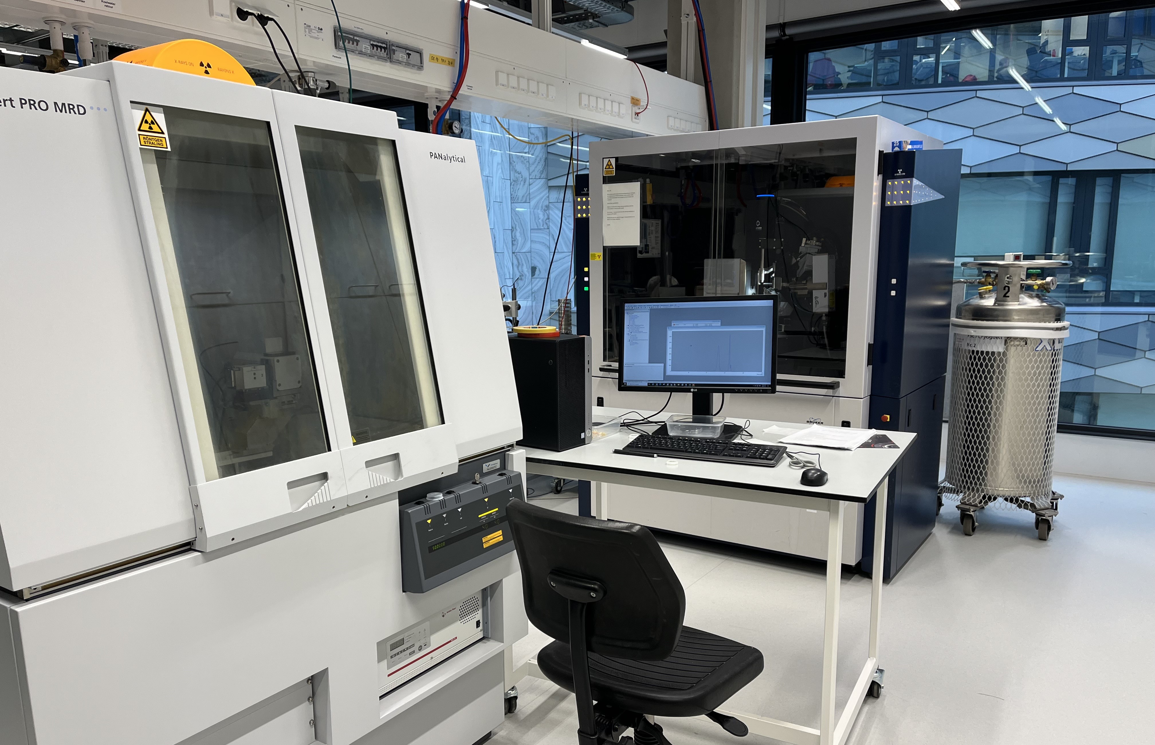
For structural characterization of thin films the MSC counts with a Philips X'pert four axes diffractometer equipped with primary and secondary optics. X-rays characteristic of Cu are generated by a PW-3373/00 (Cu LFF DK 127355) X-ray tube operated at V=40 kV and I=40 mA. In the line focus mode the beam size is ~ 12 mm x 0.4 mm. This beam is made parallel (horizontal divergence ~ 0.05°) and monochromatic by a hybrid X-ray mirror.
The spectral range of this monochromator is larger than that of the so-called four-crystal monochromators but delivers a much more intense beam, composed mainly of K1 (λ = 1.54059 Å), the K2 radiation being suppressed to less than 0.1 %. In the diffraction path an antiscatter slit, 0.04 rad Soller slits and a programmable receiving slit, are used in combination with a proportional detector. Other possibilites include point-focus mode for stress and texture measurements and the use of an analyser crystal. A heating stage (Anton Paar) is also available to heat up until 900°C under vacuum or with a N2, O2 or Ar flow.
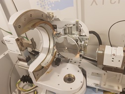
Figure 1. Panalytical Xpert MRD - thin film diffractometer.
Bruker D8 Advance. We use a Copper X-ray tube operated at 40 kV and 40 mA. It has Twin Optics for parrallel beam measurements or a motorized slits set-up as a Bragg-Bretano system and has a Lynxeye 1D stripe detector.
Bruker D8 Endeavor. Automated X-ray diffractometer for standard powder XRD measurements.
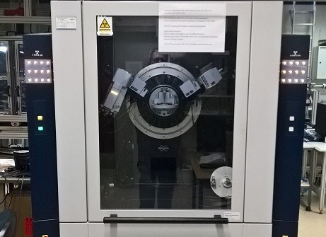
Figure 2. Bruker D8 Advance - powder diffractometer.
Figure 3. Bruker D8 Endeavor - automated powder diffractometer.
Bruker D8 Venture dual beam setup. We can either use a Molybdenum X-ray Tube or Copper High brilliance microsource with a Photon 100 2D detector. We can measure in a temperature range of 100 K - 450 K.
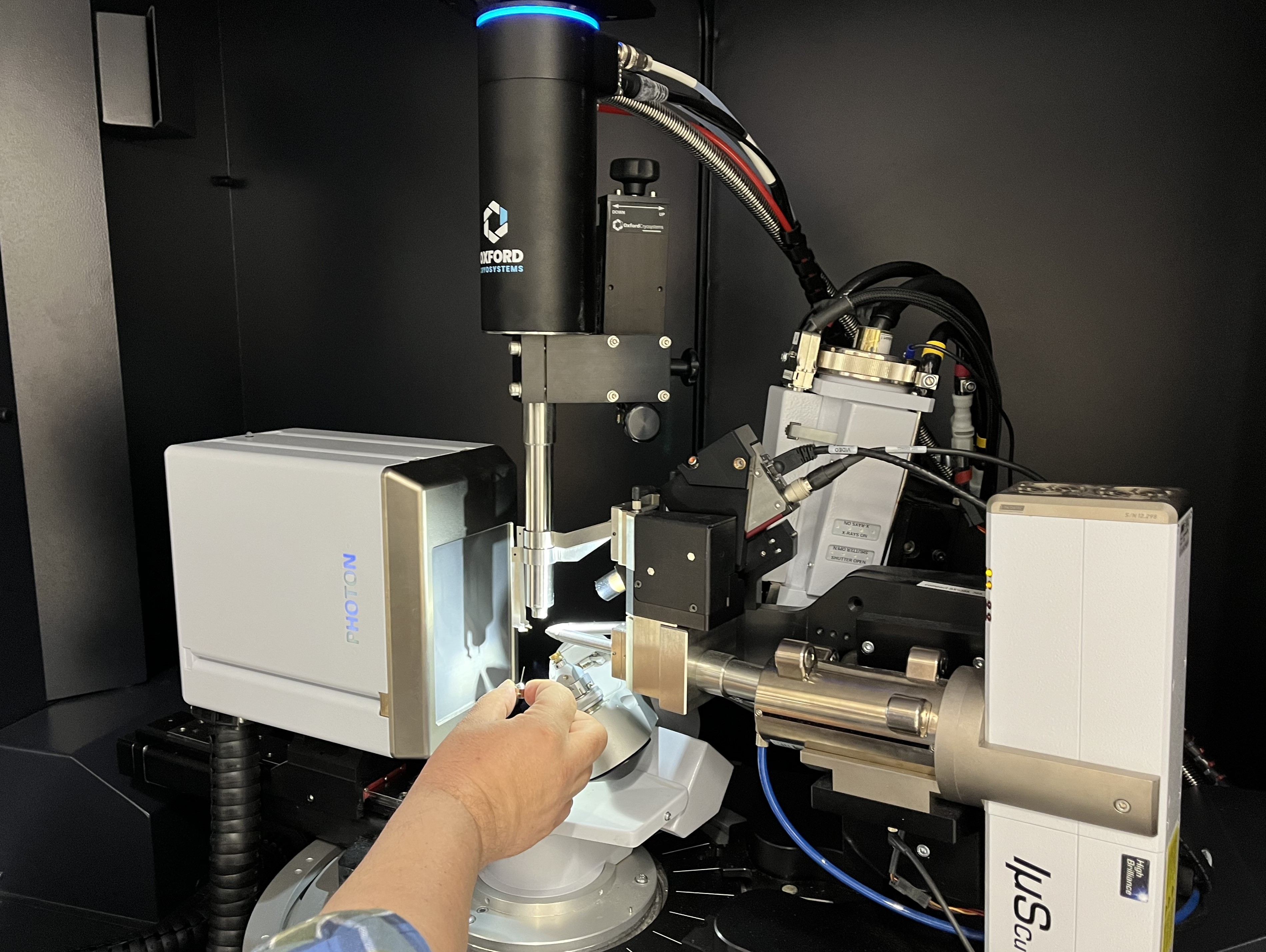
Figure 4. Bruker D8 Venture - Single crystal diffractometer.
Ferroelectric, piezoelectric, pyroelectric and electromechanical properties are measured in thin films and bulk materials using an aixACCT double beam laser interferometer and an aixACCT thin film analyser. A Radiant Precision Workstation is also available for ferroelectric loop measurements. For pyroelectric current measurements, two Keithley electrometers are also available.
Local piezoelectric, magnetic, and conductivity measurements are performed using a scanning probe microscope (VEECO Dimension V with TUNA module).
The electric field generated in a piezoelectric material per unit mechanical stress applied to it (piezoelectric voltage coefficient g) can be measured using the Universal Testing System INSTRON 5940.
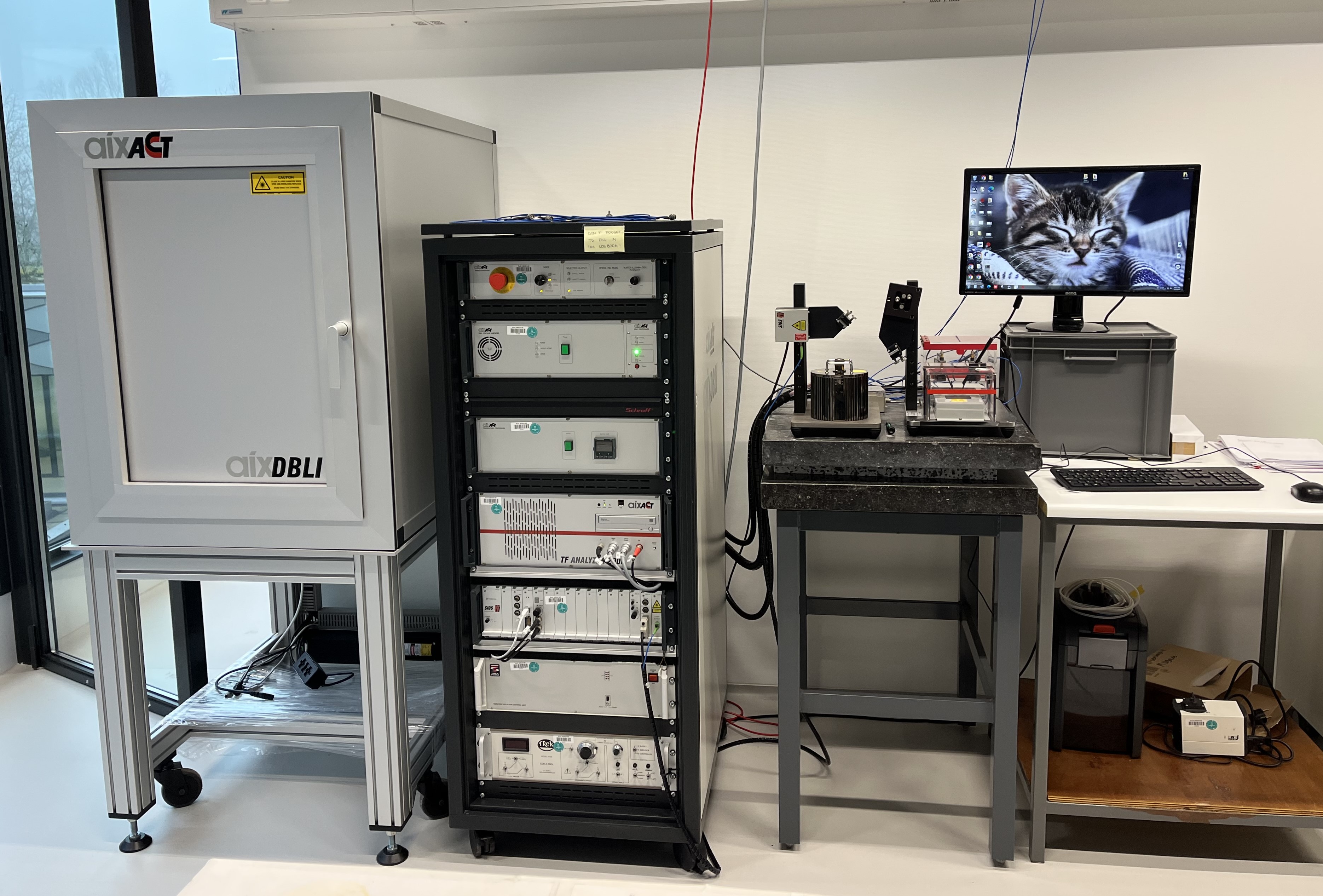
Figure 5. AixACCT System.
MPMS is a very sensitive magnetometer due to the utilization of a liquid Helium cooled SQUID (superconducting quantum interference device) to measure changes in the magnetic flux, which is converted to and measured as current, as the sample moves through the superconducting detection coil.
Our Quantum Design MPMS makes it possible to study the magnetic properties of materials at temperatures from 1.8 to 400 K under magnetic fields of up to 7 Tesla. For measurements up to 800 K, a sample space oven has been implemented. It is possible to measure materials in powder, single-crystal or pellet form.
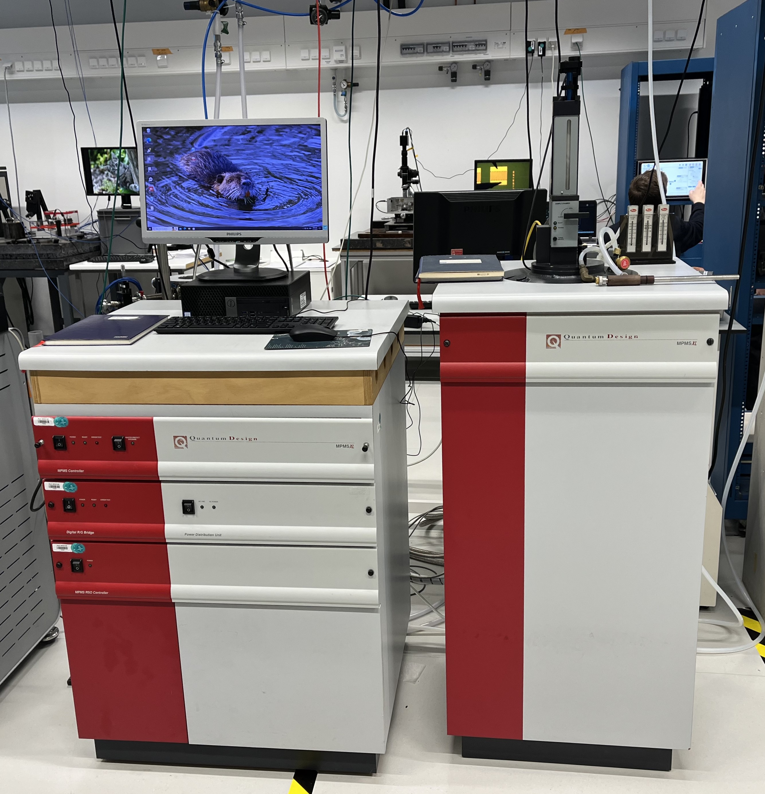
Figure 6. Quantum Design MPMS - XL 7T squid magnetometer 2 - 800K.
Physical Property Measurement System (PPMS)
PPMS is a cryogenic platform used to carry out temperature and magnetic field dependent physical measurements. Transport measurements, such as resistivity, Hall effect, Seebeck effect, magnetoresistance, as well as capacitance and magnetocapacitance, pyroelectric and ferroelectric measurements can be performed. By means of a sample rotator, it is possible to easily measure anisotropic properties of single crystal samples. The measurements are controlled by using LabView and Visual Basic programs.
Temperature range: 2 to 400 K
Maximum magnetic field: 9 T
Options:
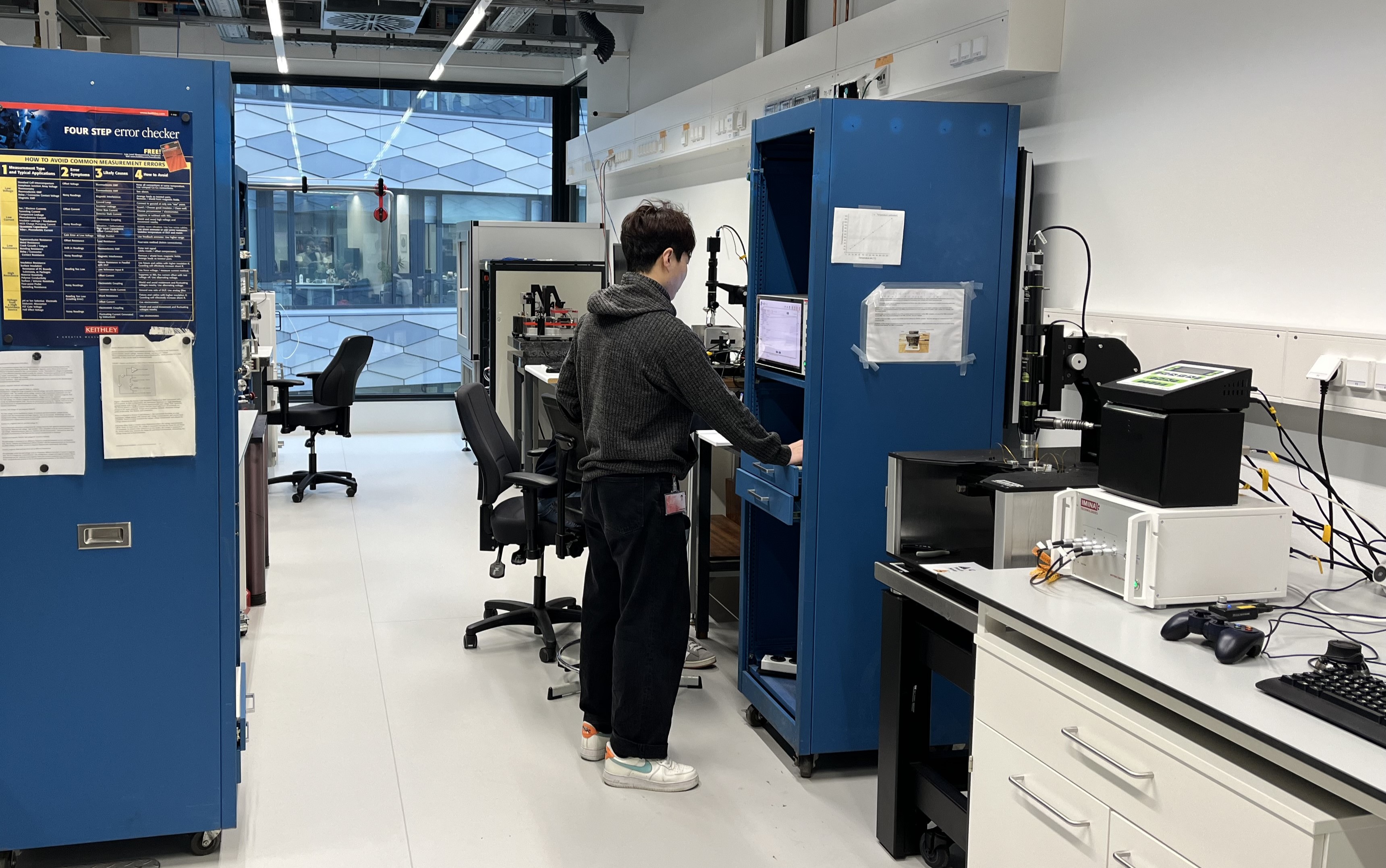
Probe Stations
Two probe stations with 4 probe micro manipulators are available:
Electrical Measurements
The electrical characterizations can be done using:
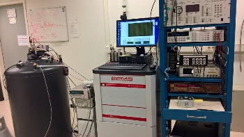
Figure 7. Quantum Design PPMS Physical Property Measurement System 9T 2-400K.
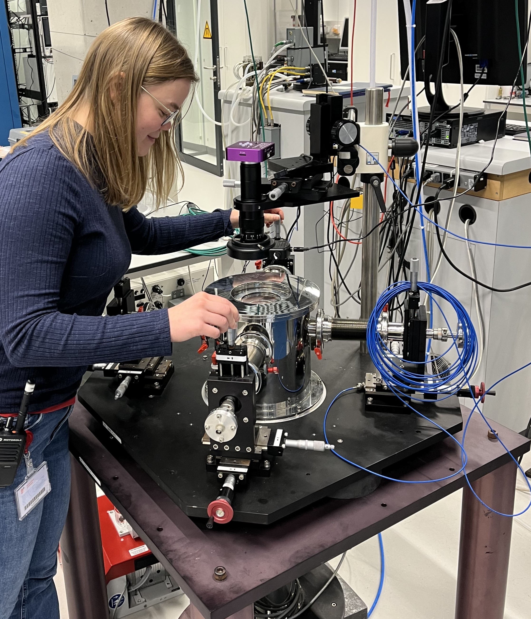
Figure 8. Janis low temperature probestation.
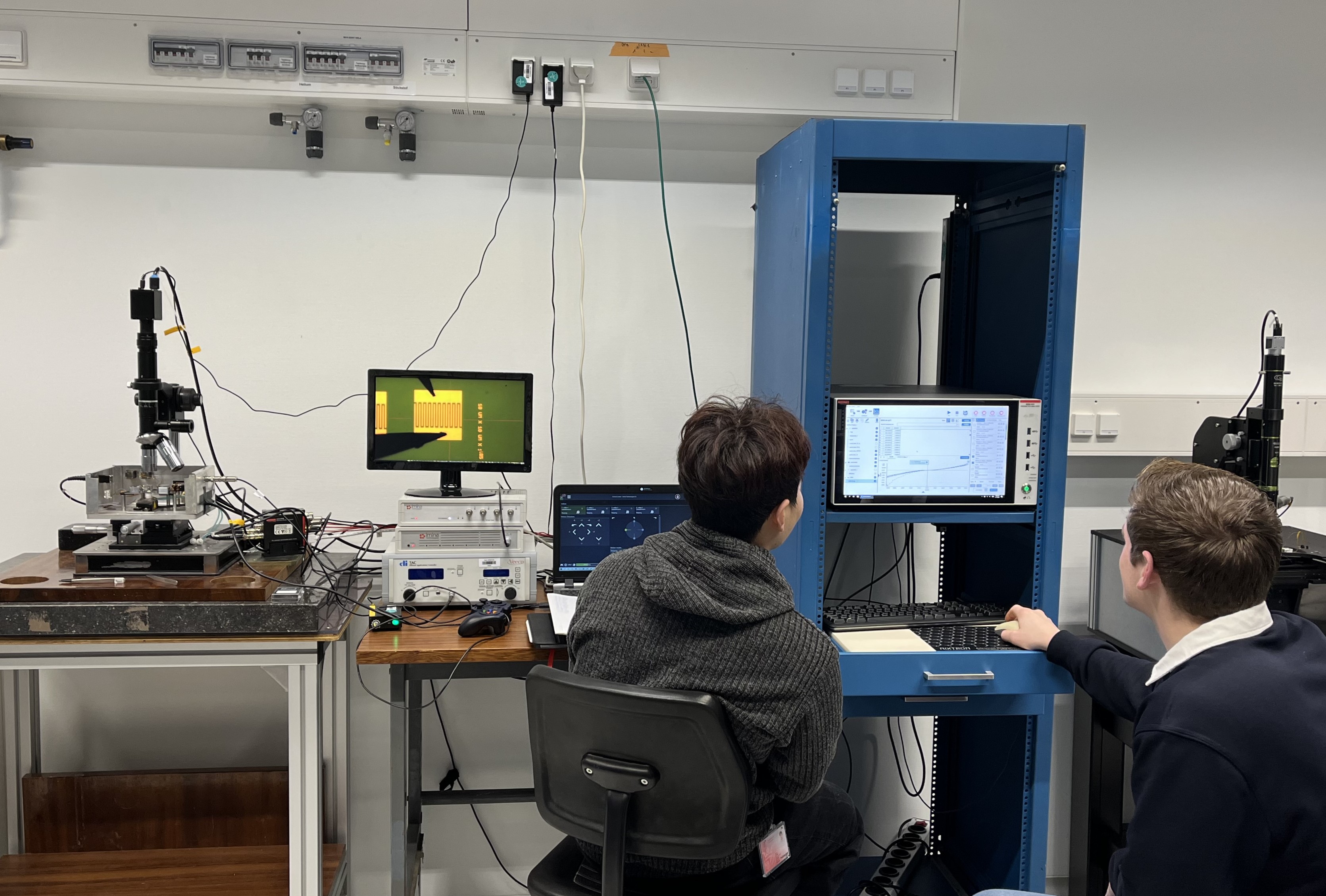
Figure 9. Keithley 4200 - SCS Parameter Analyzer.
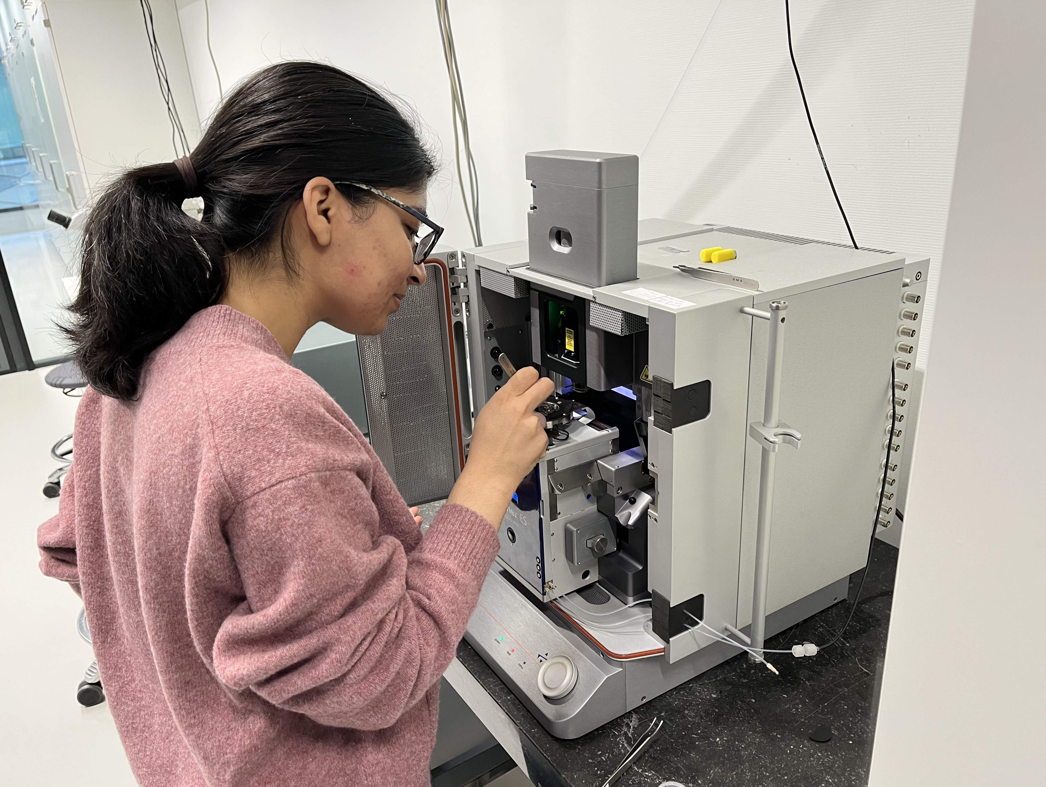
Figure 10. Cypher ES - AFM.
The study of the surfaces at the nanoscale level can be done using:
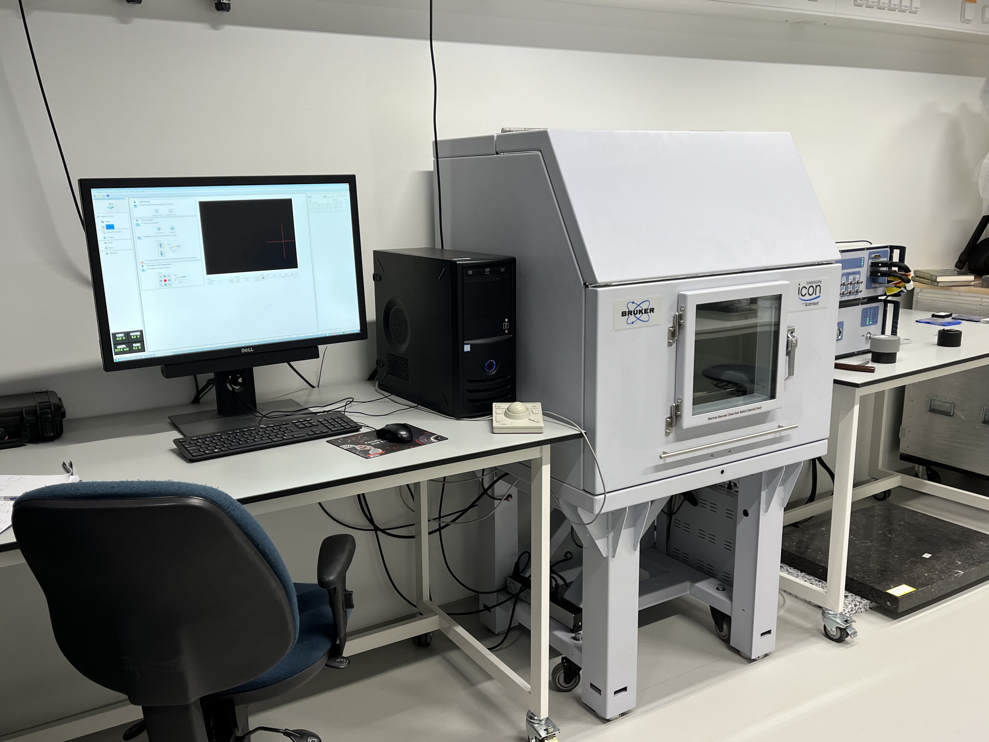
Figure 11. Bruker ICON AFM.