PROJECTS: NOHEDA GROUP

OngoingProjects  

Our mission is to develop novel materials for future electronics. Our focus is on ferroelectrics and multiferroics (for memory applications), piezoelectrics (for energy harvesting) and memristors (for adaptable electronics and neuromorphic computing).

Lines of Research

Compact Neuristors
Mart Salverda (m.salverda@rug.nl)

Developing materials that can lead to compact versions of artificial neurons (neuristors) and synapses (memristors) is the main aspiration of the nascent neuromorphic materials research field. Oscillating circuits are interesting as neuristors, as they emulate the firing of action potentials. Here we present room-temperature self-oscillating devices fabricated from epitaxial thin films of semiconducting TbMnO3. We show that the negative differential resistance regime observed in these devices, orginates from transitions across the electronic band gap of the semiconductor. The intrinsic nature of the mechanism governing the oscillations gives rise to a high degree of control and repeatability. Obtaining such properties in an epitaxial perovskite oxide opens the way towards combining self-oscillating properties with those of other piezoelectric, ferroelectric, or magnetic perovskite oxides in order to achieve hybrid neuristor-memristor functionality in compact heterostructures.

Various electrical measurements on epitaxial TbMnO3

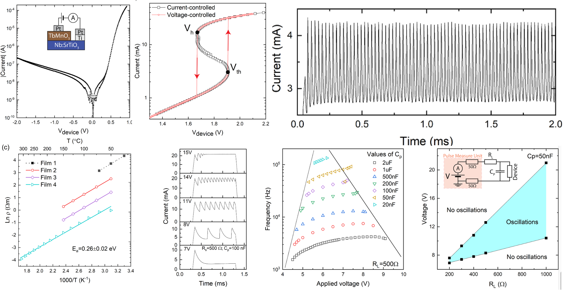
Figure 1. Various electrical measurements on epitaxial TbMnO3. [1]


Ferroelastic domain walls in BiFeO3 as memristive networks
Jan Rieck (j.l.rieck@rug.nl)

Electronic conduction along individual domain walls (DWs) has been reported in BiFeO3 (BFO) and other nominally insulating ferroelectrics. DWs in these materials separate regions of differently oriented electrical polarization (domains) and are just a few atoms wide, providing self-assembled nanometric conduction paths. In this project, we show that electronic transport is possible also from wall to wall through the dense network of as-grown DWs in BFO thin films. Electric field cycling at different points of the network, performed locally by conducting atomic force microscope (cAFM), induces resistive switching selectively at the DWs, both for vertical (single wall) and lateral (wall-to-wall) conduction. These findings are the first step towards investigating DWs as memristive networks for information processing and in-materio computing.

cAFM measurements on a BFO/STO sample with a 55 nm-thick BFO layer, measured with in-plane geometry.

Figure 1. cAFM measurements on a BFO/STO sample with a 55 nm-thick BFO layer, measured with in-plane geometry. [1]


STEMfit: statistical analysis software for transmission electron microscopy
Ewout van der Veer (ewout.van.der.veer@rug.nl)

The transmission electron microscope is one of the most powerful tools for imaging the atomic structure of materials. However, to get the most out of these instruments we need to perform statistical analyses on the images they produce. Our in-house developed software package (STEMfit) provides a platform for analyzing (S)TEM images and extracting as much useful information from them as possible. Using this software, we can now determine the positions of atoms in the images with a precision of as little as 5 pm. Using that information, we can map properties such as strain and ferroelectric polarization at large scale and single atom resolution. Download STEMfit: https://github.com/evanderveer/STEMfit

STEMfit workflow

Figure 1. STEMfit workflow. [1]


Zirconium oxide ferroelectrics for memory devices
Yulei Li (yulei.li@rug.nl)

Since the first report of robust ferroelectricity in doped HfO2 thin films in 2011, HfO2-based thin films have been the candidate material for the next generation of non-volatile memory devices due to the large remanent polarization (Pr) at the nanoscale and good compatibility with silicon-based modern microelectronics, which is of great significance for miniaturization of ferroelectric devices. Chemical modifications play an important role in the property optimization of HfO2 ferroelectrics. Hf0.5Zr0.5O2 films are prepared by different methods and demonstrate robust remanent polarization and reliable switching performance. The related ferroelectric devices are widely studied. Given that ZrO2 is cheaper and more abundant than HfO2, decreasing the use of HfO2 will increase the sustainability of this material. In this research, high quality ZrO2 nanoscale thin films are deposited by Pulsed Laser Deposition (PLD), epitaxially on SrTiO3 (STO) substrates. The polar phase, its stabilization mechanism and the buffer layer effect are investigated by XRD and TEM techniques. Capacitors are fabricated to investigate the electrical properties. The thickness limitation to obtain ferroelectric ZrO2 will be discussed. With the understanding of the switching mechanism in ferroelectric ZrO2 films, novel ferroelectric tunnel junctions (FTJ) with ultrathin ZrO2 film will be fabricated and the electrical properties will be investigated.

a)-c) Out-of-plane (left, bottom) and in-plane (right, top) device geometries. d)-e) Polarization loops in the out-of-plane (d) and in-plane (e) geometries.

Figure 1. a)-c) Out-of-plane (left, bottom) and in-plane (right, top) device geometries. d)-e) Polarization loops in the out-of-plane (d) and in-plane (e) geometries.


Epitaxial HfO2-based superlattices for enhanced ferroelectric properties
Johanna van Gent González (j.van.gent.gonzalez@rug.nl)

Hafnia (HfO2) is a CMOS-compatible ferroelectric material exhibiting spontaneous polarisation at the nanoscale, making it attractive for application in ferroelectric devices such as ferroelectric field-effect transistors (FeFET) and ferroelectric random-access memory (FeRAM). However, the mechanism by which the material is ferroelectric remains to be fully understood and stabilising the spontaneous polarisation over the device lifetime has proven challenging. To both improve and better understand the ferroelectric properties of HfO2, epitaxial superlattices of HfO2 with other binary oxides are grown by pulsed laser deposition (PLD). Such superlattices improve the stability of the ferroelectric phase of HfO2, thereby enhancing the spontaneous polarisation and durability that can be achieved in HfO2-based devices.

HfO2-ZrO2 multilayer pole figure and ferroelectric measurement

Figure 1. a) Schematic of a HfO2-ZrO2 multilayer, b)-c) pole figure and ferroelectric measurement corresponding to a twofold repetition of HfO2-ZrO2 layers.


Nickelates as memristive devices
Foelke Janssen (foelke.janssen@rug.nl)

Nickelates are part of the group of phase change materials. They switch from an insulating state at lower temperature to a metallic state at higher temperature. The insulator to metal transition can be tuned by many parameters such as strain, doping or oxygen vacancies. In this work we are investigating how the transition from a metallic to an insulating state by the intercalation of different ions in a nickelate thin film can be used for memristive devices.

Project visual abstract

Figure 1. The conductance change in a SNO/LSMO thin film stack at different temperatures and for different pulse-train times.


Epitaxial BaTiO3 films for memristive devices
Jingtian Zhao (j.zhao@rug.nl)

The control of the strain state in epitaxial thin films enables the change of the crystal symmetry of materials and the associated properties, such as their polarity, electromechanical, optical, magnetic or transport properties. In my work, pulsed laser deposition is used to tune the strain state of ferroelectric BaTiO3 (BTO) thin films by the use of a buffer layer of Y-doped SrSnO3 (SSO) thin films on single crystals of SrTiO3 (STO), used as substrate. This allows the polarization of the ferroelectric to be gradually changed, which is not possible by the current method. The final goal is to fabricate ferroelectric field effect transistors (FeFET) that behave as artificial synapses with the ability to both store and process information.

Project visual abstract

Figure 1. a) Schematic of pulsed laser deposition. b) BTO/SSO/STO(100) stack. c) Schematic of a FeFET. d) Schematic of a neural network.


Electrostatic frustration for tunable volatility in ferroelectric thin films
dr. Martin Sarott (m.f.sarott@rug.nl)

Emulating the functionality of biological synapses and neurons using artificial devices requires the development of materials exhibiting volatile, non-volatile, as well as hybrid volatile/non-volatile switching characteristics. Ferroelectric materials, characterized by an inherently non-volatile electric polarization, have attracted considerable attention to mimic artificial synaptic devices, however, tuning the volatility of ferroelectric polarization switching to widen the scope of ferroelectrics for neuromorphic computing has remained largely unexplored. In this project, we investigate the design of epitaxial ferroelectric heterostructures with a tunable electric field response between fully volatile and fully non- volatile by leveraging polar discontinuities at the top and bottom interfaces of the functional ferroelectric layer. Acting on the electrostatic boundary conditions in this manner will allow us to tailor the depolarizing field, the stability of the ferroelectric polarization, and, in turn, the volatility of the electric-field response.

Tailoring the remanence of the ferroelectric polarization to emulate artificial neurons
and synapses.

Figure 1. Tailoring the remanence of the ferroelectric polarization to emulate artificial neurons and synapses.


Anything pique your interest?